Semiconductor
Mid-end Inspection
-
Integrated Measurement System
Semiconductor Mid-end
Visual Inspection -
INTEKPLUS's WSI (White Light Scanning Interferometer) 3D optical system is an optimal inspection solution for fine pitch bumps required for high-end products. FC-Substrate, FO-PLP, Wafer, and the performance of the equipment have been verified through bump inspection of various products.
INTEKPLUS is responding by partnering with global leader companies that are continuing various trials and developments, and the experience is the best Spec. It is becoming the foundation for realizing further customer satisfaction.
- Package Substrate Bump AOI
- From high-end products that require high inspection performance for fine pitch to middle-end products that increase productivity, global leaders have chosen INTEKPLUS's BAOI for FC-Substrate.
-
Inspection Targets
FC-BGA, Panel, FC-CSP
-
Inspection Items
Bump Height, Bump Area Warpage, Bump Coplanarity, Thickness Valuation, Bump Diameter, Etc.
-
Model
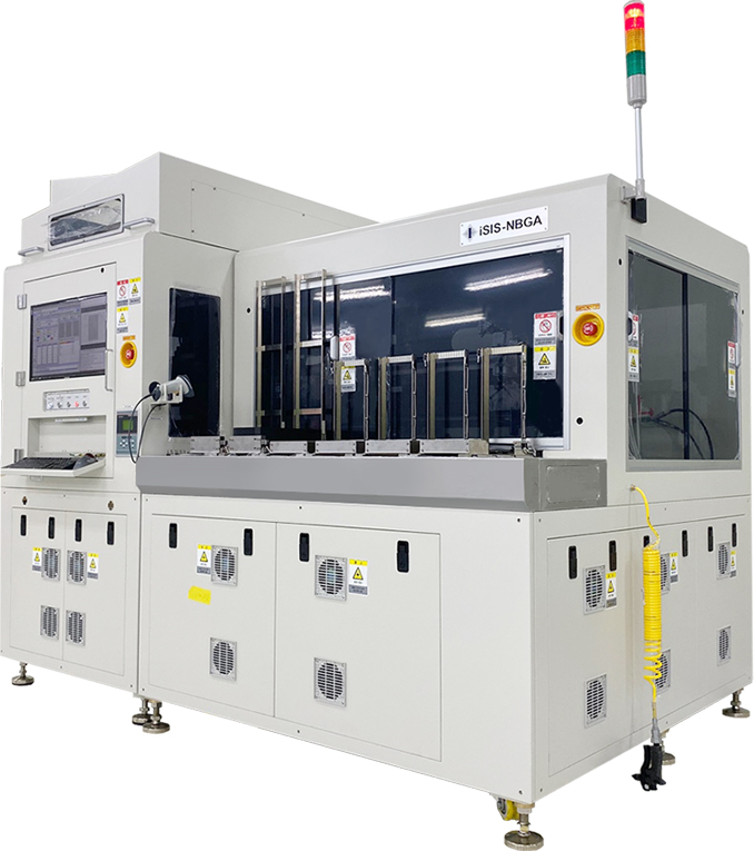
iSIS-NBGA (In-tray inspection for Flip-chip BGA)
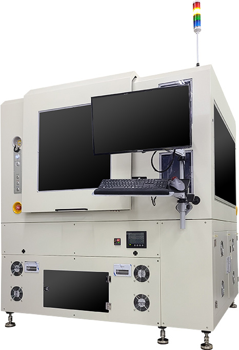
iSIS-NTV (Suction jig inspection for Flip-chip BGA)
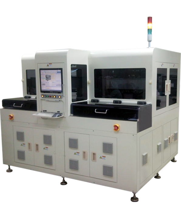
iSIS-QPM(Full-Panel/Q-Panel inspection)
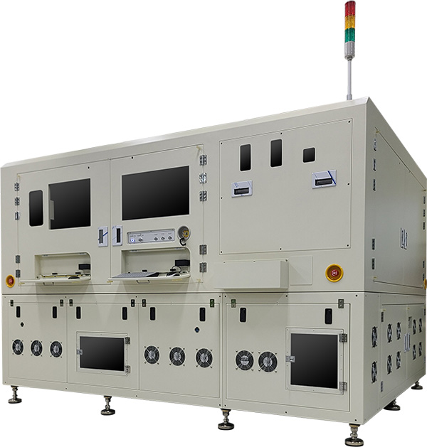
iSIS-NCSP (Flip-chip CSP inspection)

-
- 3D Method
- WSI
-
- Height Accuracy
- ±1µm
-
- Inspection Stage
- In-Tray

-
- 3D Method
- WSI
-
- Height Accuracy
- ±1µm
-
- Inspection Stage
- 3D on Suction jig
-
- 3D Method
- WSI
-
- HeightAccuracy
- ±1µm
-
- L/UL
- Manual / EFEM
-
- 3D Method
- WSI
-
- Height Accuracy
- ±1µm
-
- Inspection Stage
- Suction jig
- Wafer / PLP Bump AOI
- For wafers, especially PLP, each company has its own process. INTEKPLUS's equipment is not only high in Resolution Spec., but also has proven inspection performance on various types of surfaces.
-
Inspection Targets
FC-BGA, Panel, FC-CSP
-
Inspection Items
Bump Height, Bump Area Warpage, Bump Coplanarity, Thickness Valuation, Bump Diameter, Etc.
-
Model
iSIS-FP3D (Wafer, PLP inspection)
-
- 3D Method
- WSI
-
- Height Accuracy
- ±1µm
-
- L/UL
- Manual / EFEM